Audio Sound System

Breaking

Wednesday, April 22, 2026

Bass Booster Circuit with Low Pass Filter utilizing JRC4558

April 22, 2026 0
Bass Booster Circuit with Low Pass Filter utilizing JRC4558

Introduction

A low pass filter circuit Bass Booster is an essential component in audio systems that enhances the bass frequencies of an audio signal. The JRC4558 IC, an integrated circuit, is widely used in low pass filter circuits due to its superior performance and versatility. This circuit is known for its ability to isolate low-frequency sounds and eliminate high-frequency noise, resulting in an improved audio experience. In this article, we will explore the functioning of the low pass filter circuit Bass Booster using the JRC4558 IC, highlighting its unique features and benefits.

When we listen to music or any sound, there are instances where we feel vibrations or shaking either within ourselves or objects in our surroundings. These vibrations are caused by low or bass sounds, which have frequencies ranging from 25Hz to 150Hz. Sounds beyond these frequencies are considered mid or high frequencies. In this article, we provide you with a low pass filter Bass-Booster circuit that covers frequencies from 20Hz to 150Hz, ideal for subwoofers.

If you’re in need of a circuit that specifically focuses on low audio frequency (bass), then this JRC4558 low pass filter bass-booster circuit is perfect for you! It effectively removes high frequencies from audio, leaving only the low frequencies between 25Hz and 150Hz.

Given that audio frequencies are categorized into different ranges such as low, mid, and high frequencies (Hz to KHz), it seems like you are interested in cutting off the high frequencies and focusing solely on the low frequencies. This Low Pass Filter Bass-Booster circuit will help you achieve that.

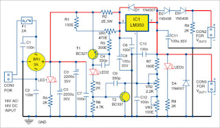
Circuit Diagram of Low Pass Filter Bass-Booster

This project can be designed using a few basic components. The circuit diagram of this project is shown below.

Bass Booster Circuit with Low Pass Filter utilizing JRC4558

Components List of Low Pass Filter Bass-Booster

Following is the list of all components used in this project:

  • JRC4558 IC x 1
  • 1KΩ Resister x 3
  • 5KΩ Resister x 1
  • 10KΩ Resister x 3
  • 51KΩ Resister x 1
  • 22µF Capacitor x 2
  • 100nF Capacitor x 1
  • 0.63pF Capacitor x 1
  • 150nF Capacitor x 1

Working Explanation of Low Pass Filter Bass-Booster

The output of this circuit is connected to the input of a subwoofer amplifier, which is responsible for driving the subwoofer speaker. The circuit is built around the op-amp integrated circuit JRC4558 and utilizes a dual rail power supply, consisting of positive and negative rails as well as a ground (GND) connection.

Conclusion

In conclusion, the low pass filter circuit Bass Booster utilizing the JRC4558 IC is a highly effective solution for enhancing the bass frequencies in audio systems. Its ability to eliminate high-frequency noise while isolating low-frequency sounds ensures a superior audio experience. By incorporating this circuit into audio systems, users can enjoy a more robust and immersive bass output. The JRC4558 IC’s versatility and superior performance make it a popular choice for audio signal processing, providing reliable and high-quality bass enhancement. With its unique features and benefits, the low pass filter circuit Bass Booster using the JRC4558 IC proves to be an essential component in achieving exceptional sound reproduction.

More projects, You may like:

For more project and circuit diagrams, you can go through the Schematics in the main menu where you can find many interesting projects and circuit diagrams like audio amplifier circuits, voltage booster circuitbattery charger circuit and timer circuits etc., which are all beginner circuit projects. Feel free to check them out!

Friday, April 17, 2026

18W Car Stereo Amplifier Circuit Diagram

April 17, 2026 0
18W Car Stereo Amplifier Circuit Diagram

This automobile stereo amplifier project is a class AB audio power amplifier using the Hitachi HA13118 module. It not only can be used in automobile application but also in any transportable or home amplifier process. It is simple to construct & has a maximum of outside parts. The module has a high power output from a low voltage supply using the bridge tied load system, & a high gain of 55dB.

This project will be useful in applications where the input signal is a low level, without requiring the use of a separate pre-amplifier. This IC module has a built in surge protection circuit, thermal shutdown circuit, ground fault protection circuit & power supply fault protection circuit making it reliable.
The Specifications of this project 
D.C. Input : 8 – 18V at 1-2 A

Power output : 18W maximum, 4 ohm load, 18V DC supply

S/N ratio : > 70 dB

THD : < 0.2% @ 1W

Freq. Response : ~ 30 Hz to 30 kHz, –3 dB

Input level : < 25 mV, for full output (G > 50dB)

Input Impedance : ~ 30 k ohm

The supply voltage necessary for this project is 8 -18V DC, at least one to two Amps. Maximum output power will only be obtained with a power supply of 18V at greater than two A, using a four ohm speaker. The power supply ought to be well filtered to reduce mains hum, a regulated supply will reduce noise even further. Additional filtering is unnecessary if operating from a battery supply.

Circuit Diagram Description

Most of the circuitry is contained within the amplifier module. C10 is the input coupling capacitor and blocks DC from the input. C11 bypasses any RF which may be present at the input. C1 & C2 provide an AC ground for the inverting inputs of the IC. R1/C7 and R2/C8 provide a high frequency load for stability with difficult speakers. C five & C six provide bootstrap feedback for the IC. C9 & C12 provide power supply filtering.

18W Car Stereo Amplifier Circuit Diagram

18W Car Stereo Amplifier Circuit Diagram


An externally mounted logarithmic potentiometer of between 10k ohm and 50k ohm, is used depending on the desired input impedance. The impedance ought to be keep as high as feasible for a guitar amp, unless using a separate pre-amp. Make sure-that the heat sink is mounted to the module.

5 Watt Amplifier with IC AN7147 (Surround)

April 17, 2026 0
5 Watt Amplifier with IC AN7147 (Surround)

The 5-Watt amplifier circuit with surround system below is worth a try if you're looking to build a low-power, relatively inexpensive amplifier. This amplifier can be used in your audio equipment or simply for a test drive. Below is the amplifier circuit:

5Watt Amplifier with IC AN7147 (Surround)
Schematic Image of 5Watt Amplifier with IC AN7147 (Surround)

 The AN7147, along with a few additional components, can represent a simple surround sound system that requires no opamps or negative voltage supplies. As shown in the  schematic Mini Amplifier Circuit With Surround System, A basic stereo amplifier is transformed into a surround sound system using a trick called "adding feedback from the opposite channel." When surround sound is required, the negative feedback signal provided by C13 and C12, R3, and R4 is fed to the input of the other amplifier. The resulting phase difference creates the surround effect. When surround sound is not required, the effect can be disabled by pressing switch S1. This causes the bistable circuit built around IC2.A and IC2.B to switch and drive transistors T1 and T2, effectively driving the negative feedback signal to ground. A high-efficiency LED and a 3.3 kΩ series resistor (R14) must be used to ensure the maximum output of the CMOS 4001 device is not exceeded. The amplifier should not be loaded with an impedance less than 3Ω.

Thursday, October 9, 2025

Power Amplifier TDA2040

October 09, 2025 0
Power Amplifier TDA2040

Description:
This circuit uses the TDA2040 IC as the main part of a class AB audio amplifier that can produce up to 25 watts of power when connected to a 4-ohm speaker. The TDA2040 is famous for being efficient, having low distortion, and staying cool during use. It works well for small music systems, active speakers, or homemade audio projects that need clear and strong sound.

Introduction

In the field of audio electronics, sound quality and efficiency are always key considerations. One widely used component in power amplifier design is the TDA2040 IC. Created by STMicroelectronics, this IC is a monolithic class AB amplifier that includes built-in protection features such as thermal overload and short circuit protection.

The TDA2040 has a straightforward and efficient design that needs just a few extra parts, such as resistors and capacitors, to work best. It can produce about 25 watts of power when connected to a 4-ohm load, making it a great choice for home audio setups, small guitar amplifiers, or portable speaker builds.

This article explains in detail the working principle, circuit design, and component list of the 25W power amplifier using TDA2040, along with assembly tips and testing methods for best results.

Circuit Diagram

Figure: 25W Power Amplifier using TDA2040

Power Amplifier TDA2040

Circuit Explanation

This circuit is configured as a non-inverting amplifier, where the input signal is fed to pin 1 (non-inverting input) of the TDA2040. The amplified output is taken from pin 4, while pin 3 is connected to ground. The positive supply voltage is connected to pin 5.

1. Input Stage

The input signal passes through a 2.2µF coupling capacitor that blocks DC and allows only the AC (audio) signal to pass. The 22kΩ resistor connected to ground serves as a bias resistor to stabilize the input voltage.

A combination of 22µF capacitor and 680Ω resistor in the feedback path forms a frequency compensation network to maintain low-frequency stability and prevent oscillation.

2. Feedback Network

The feedback path runs from pin 4 (output) to pin 2 (inverting input) through a 22kΩ resistor and a 680Ω resistor. This determines the amplifier gain, calculated by:

Gain = 1 + (Rf / Ri)
Gain = 1 + (22000 / 680) ≈ 33.4

This means the input signal is amplified about 33 times, making it suitable for sources like mobile phones, DACs, or preamps.

3. Power Supply Filter

The amplifier operates with a single supply voltage +Vs (typically between +18V to +22V DC). The 220µF and 100nF capacitors act as filters to remove supply noise and stabilize voltage during signal peaks.

4. Output Stage

The output from pin 4 passes through a large 2200µF capacitor before reaching the speaker. This capacitor blocks DC from reaching the speaker. A 2.2Ω resistor and 100nF capacitor in parallel form a Zobel network to maintain stability with inductive loads like speakers.

5. Additional Components

The 22µF capacitor on the inverting input enhances low-frequency response (bass). The TDA2040 also includes built-in protection such as:

  • Thermal shutdown (overheating protection)
  • Short-circuit protection
  • Safe Operating Area (SOA) protection

Component List

ComponentValueFunction
ICTDA2040Main power amplifier
R122kΩFeedback resistor
R2680ΩGain resistor
R322kΩInput bias resistor
R42.2ΩZobel resistor
C12.2µFInput coupling capacitor
C222µFLow frequency compensation
C322µFFeedback capacitor
C4100nFSupply filter (HF)
C5220µFSupply filter (LF)
C62200µFOutput coupling capacitor
C7100nFZobel capacitor
Speaker4–8ΩLoad
Power Supply+18V to +22V DCDC source

Working Principle

  1. The input audio passes through C1 and enters pin 1 of the IC.
  2. TDA2040 amplifies the signal about 33 times.
  3. The amplified signal is available at pin 4 and passes through C6 to the speaker.
  4. The RC network at output ensures load stability.
  5. Filter capacitors maintain supply voltage stability.

Assembly and PCB Tips

  • Mount a large heatsink on the TDA2040 to prevent overheating.
  • Keep input and output traces separate to avoid parasitic feedback.
  • Place the 100nF and 220µF capacitors close to the IC supply pins.
  • Use thick wires for the speaker output to reduce power loss.
  • Double-check capacitor polarity before powering the circuit.

Testing Procedure

  1. Check all connections carefully before applying power.
  2. Use a regulated +18V DC supply (or transformer 18V-0V-18V with rectifier).
  3. Connect an audio source (phone, MP3 player) and slowly raise volume.
  4. If there is no hum or distortion, the amplifier works correctly.
  5. Measure output with a multimeter or oscilloscope — you should get around 25W RMS on a 4Ω load.

Advantages and Disadvantages

Advantages:

  • Simple and easy to build
  • Clean sound with low distortion (THD < 0.1%)
  • High output power up to 25W RMS
  • Built-in thermal and short-circuit protection
  • Low cost and widely available components

Disadvantages:

  • Requires a large heatsink
  • Not suitable for high-power (>50W) systems
  • No built-in tone control (bass/treble)

Additional Tips

  • Add a preamp tone control for better sound clarity.
  • Use shielded cables for the input to avoid hum and noise.
  • Build two identical circuits for a stereo amplifier.
  • Use a toroidal transformer (18V 3A) and filter capacitors above 4700µF for best results.

Conclusion

The 25W Power Amplifier using TDA2040 is an excellent project for audio enthusiasts who want high-quality sound with simple construction and low cost. Its balance of output power, efficiency, and protection features makes it a popular choice for DIY audio builders.

With only a few components, you can enjoy clear and powerful audio for home, workshop, or portable use. Hopefully, this guide helps you understand how the TDA2040 works and inspires your next audio project.

Thursday, February 22, 2024

A Basic Electronic Bagpipe Music Generator Circuit

February 22, 2024 0
A Basic Electronic Bagpipe Music Generator Circuit

A Basic Electronic Bagpipe Music Generator Circuit


Introduction

Have you ever wanted to learn how to play the bagpipes but thought it was too intricate or costly? Thanks to this electronic bagpipe circuit, you can now immerse yourself in the mesmerizing sounds of bagpipe music with ease.

Prepare yourself to enter a realm of pure imagination where the classic sounds of a traditional bagpipe are recreated through an easy-to-assemble electronic circuit. Discover our simple electronic bagpipe circuit that generates an accurate dual-tone drone sound!

The Music Generator Circuit will need the following hardware.

Music Generator Circuit Hardware


Monday, February 6, 2023

LA4440 Audio Amplifier Circuit

February 06, 2023 0
LA4440 Audio Amplifier Circuit

LA4440 Audio Amplifier:

The LA4440 is an integrated circuit (IC) designed as a dual audio power amplifier. It is frequently utilized in audio amplifiers and various electronic devices that need audio amplification. To verify the proper functioning of the LA4440, you should test it by measuring its output voltage and comparing it to the anticipated values across different loads and input signals. Furthermore, conducting a visual inspection of the device for any physical damage or indications of overheating is also advisable.


LA4440 Audio Amplifier Circuit

A straightforward audio amplifier built on the LA4440 IC. This will take the headphone output level from your computer and enhance it to power a pair of external speakers. If you are enjoying music or films on laptops In the realm of computers, this is a minor project that proves beneficial to you. The speakers on notebooks are seldom powerful enough to provide a satisfying listening experience. While they allow users to hear audio, they fall short for anything resembling music or movie soundtracks, resulting in a subpar output of a laptop the volume integrated into the speakers is insufficient, and this LA4440 Audio Amplifier Circuit addresses that low power with some extra amplification.

If you need to diagnose an issue with the LA4440, Here are several steps you can take:

  1. Verify the input voltage: Ensure that the input voltage supplied to the LA4440 falls within the designated range for the device.

  1. Verify the load impedance: Confirm that the load impedance linked to the LA4440 falls within the designated range.

  1. Verify the supply voltage: Ensure that the supply voltage to the LA4440 is consistent and falls within the designated range. An unstable supply voltage may lead to performance issues with the device.
  1. Verify the thermal management: Ensure that the LA4440 is sufficiently cooled and has proper ventilation to release heat. Excessive heat can lead to irreversible damage to the device.
  1. Check the wiring: Check the wiring and connections between the LA4440 and other components in the circuit to ensure that there are no loose connections or short circuits.
  1. Check the input signal: Ensure that the input signal to the LA4440 is within the specified range and is of good quality. A noisy or distorted input signal can cause problems with the performance of the device.
These are just a few steps you can follow to troubleshoot a problem with the LA4440. If you are still having trouble, it may be best to consult the datasheet for the device or seek the assistance of a qualified technician.

Friday, February 21, 2020

Power Supply For Adjustable Voltage And Current

February 21, 2020 0
Power Supply For Adjustable Voltage And Current
How to make a Power Supply For Adjustable Voltage And Current, The circuit diagram of the power supply is shown in Fig. 1. It is built around bridge rectifier (BR1), adjustable voltage regulator LM350 (IC1), transistors BC327(T1) and BC337(T2), and a few other components.

Circuit diagram of the simple power supply with adjustable voltage and current with LM350

Fig. 1: Circuit diagram of the simple power supply with adjustable voltage and current with LM350

Input to connector CON1 can be AC or DC. If you use an 18 to 20Vrms transformer with 2A current ratings, you can have output voltage VOUT1 from 1.2V up to around 16.5V available at CON3, and VOUT2 from 0V to 15V available at CON2. Input is protected with 2A fuse F1. Capacitors C3 and C5 (2200µF) are the main filtering capacitors.

Input voltage is limited by maximum input voltage of IC LM350. Maximum power dissipation of LM350 is around 25W.


According to the data sheet, input voltage of LM350 can be from around 4.5V to 35V, and output voltage can be adjusted from 1.2V to 33V; however, we need output voltage lower than 17V.

Output voltage VOUT1 can be calculated using the following relationship:
VOUT1=1.25V (1+(VR2+VR3)/R7))

Output voltage VOUT2 is around 1.5V lower than VOUT1, and can consequently start from 0V.

Transistors T1 and T2 are implemented for adjustable current-limiting function along with potentiometer VR3. Minimum output current is around 0.35A, and depends on resistors R2 and VR3.

Wiper of VR3 should be at the right-most position to get minimum output current, and at the left-most position for maximum output current. Maximum output current is around 2A. When VR1 is adjusted for maximum output current, T1 and T2 will be on, and LED2 will glow. Otherwise, T1 and T2 will be off, and the LED2 will also be off.


Capacitors C4 and C9 prevent oscillations of T1 and T2 during transitional phases. Output voltage is adjusted with VR1 and VR3. VR2 is used for coarse adjustment, while VR3 is used for more precise output voltage adjustment.
Construction and testing

A PCB layout for this power supply circuit is shown in Fig. 2 and its component layout in Fig. 3. Assemble the circuit on the designed PCB or veroboard. Connect around 18 to 20Vrms input to CON1. Glowing of LED1 indicates the presence of power supply in the circuit. LED2 glows when higher current is taken from the load. LED3 glows when outputs are available at CON2 and CON3.

PCB layout of the simple voltage adjustable power supply

Fig. 2: PCB layout of the simple voltage adjustable power supply

Components layout for the PCB

Fig. 3: Components layout for the PCB


Measure outputs across CON2 and CON3 using a voltmeter. You should be able to get output voltage VOUT1 from 1.2V up to around 16.5V, and VOUT2 from 0V to 15V depending on positions of VR2 and VR3.


Author : Petre Tzv Petrov Sourced By EFY

Thursday, July 4, 2019

Balanced Preamp Electret Microphone Circuit Diagram

July 04, 2019 0
Balanced Preamp Electret Microphone Circuit Diagram
Among the tasks solved with the help of electret microphones, one can distinguish the sound of large rooms (for example, conference rooms, temples, etc.) with a relatively large distance from the sound source, which requires high sensitivity and noise immunity. Industrial microphones for such purposes are quite expensive and, in addition, require an autonomous power source for the preamp.

The purpose of this development was to reduce the cost of manufacturing a highly sensitive and noise-proof microphone, without significant loss of playback quality.

The basis is the scheme [1] of a balanced preamplifier, powered directly from phantom power (+48 V) of a mixing console:

Balanced Preamp Electret Microphone Circuit Diagram

Its main disadvantage is excessive amplification, leading to clipping of the microphone-sensitive microphone inputs of the console. In addition, the electret microphone supply [2] is not rational enough, as well as the temperature-dependent displacement of the transistor bases on six diodes included as stabistors. The presence of these diodes, as well as electrolytic capacitors, increases the size of the board and does not contribute to miniaturization.

An attempt to replace diode stabilization with a reverse-shifted base-emitter junction of a planar transistor (KT315) was unsuccessful due to the increased noise (hiss) in the useful signal.


Therefore, in the subsequent stabilization was applied on the shunt regulator TL431, which demonstrated the practical absence of extraneous noise and high thermal stability of the bias voltage.

The final circuit of the electret microphone preamp is shown below.


Its features were additional collector resistors R7 and R9, about 4.5 times lowering the amplitude of the signal at the connector pins compared to the collectors of transistors VT1 and VT2, as well as setting the bias base VT2 directly from the divider connected to the control electrode of the shunt DA1 (+2.5 V). The electret microphone is powered from the cathode DA1 through the divider R3R6, so that the constant voltage on it is half the power supply (ie, +2.5 V from +5 V) and becomes equal to the voltage on the control electrode DA1. Such a microphone connection provides maximum sensitivity. It was tested in the project [3] and demonstrated its practical applicability.

The diagram is made on surface-mounted components (SMD) on a printed circuit board with dimensions 37 x 15 mm (drawing in * .lay7 format is given in the attachment):


The setting is reduced to equalizing the potentials between the contact points (shown by an arrow), which are displayed on the front side of the board by rotating the trimming resistor slider.


 Search Related:

electret microphone preamp
electret microphone preamp circuit
electret condenser microphone preamp
electret condenser microphone preamp circuit
electret microphone preamp ic
electret microphone preamp kit
best electret microphone preamp
preamp mic electret
diy electret microphone preamp
preamp for electret microphone
electret microphone preamp schematic